Stay ahead of the semiconductor technology curve
As technology rapidly advances, and consumers demand more customization, Amkor has taken the next step forward in packaging with the development of new technologies to enhance, and sometimes drastically change, the packaging arena.
With one of the strongest R&D teams in the industry and over 300 leading semiconductor packaging technologists, Amkor is focused on design and development efforts to further advance the value of packaging and provide the total solution for our customers.
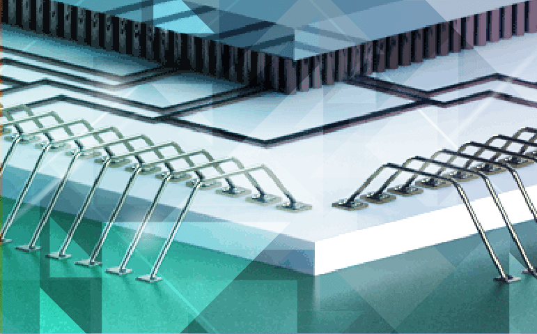
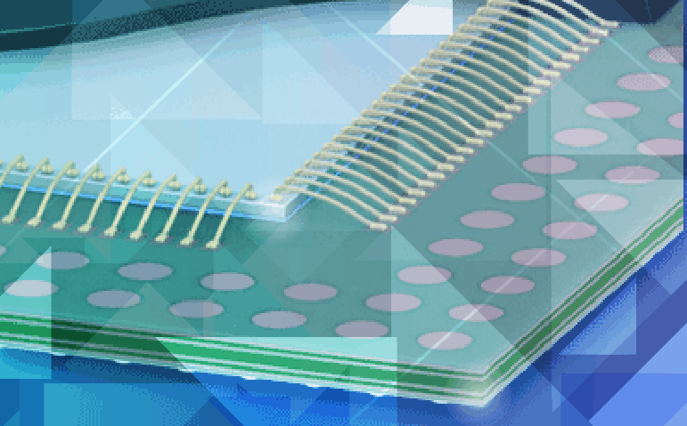
We have been instrumental in the development of almost every new packaging technology advance, including thin package formats and BGA packages. Amkor is now focusing on developing technology such as Through Silicon Via (TSV), Through Mold Via (TMV®), System in Package (SiP), copper wirebond, copper pillar, and improving interconnect with flip chip technology and 3D solutions like stacked die packages. We also have teams focused on the latest industry developments including packaging options for the emerging markets of photonics, MEMS, optical sensors,wafer-level packagingand Antenna in Package/Antenna on Package.