패키징의 전도성 밀도 증가

宽带隙半导体技术给功率封装带来了新的挑bob软件战和机遇。与硅mosfet相比,碳化硅(SiC)和氮化镓(GaN)具有更高的优值(FOM),并且扩展了功率电子器件的效率、输出功率和/或开关频率范围和工作温度范围。
With lower losses, a given size power device can control higher power loads. For example, with GaN power transistors, a power system can have ¼ the size, weight and efficiency losses compared to a silicon-based system. GaN technology can solve the system challenges from the low power (50W) end to medium and even high-power levels in wireless systems and more. Its acceptance in 5G applications makes it well-positioned for sophisticated low to medium power packaging. Similarly, SiC has power control capabilities beyond those of Si MOSFETs and requires advanced packaging for many applications. The gains and advantages in WBG devices need new packaging options to maximize the value of the entire power system.
如今的分立电源封装仅限于夹子、导线和焊接接口的电气性能。一般来说,离散封装遵循的设计理念是,更大的尺寸/体积与更高的功率处理能力相关。然而,这些更有效的晶体管技术提供了在相同尺寸的封装中处理更多功率或显著降低形状因子的能力。
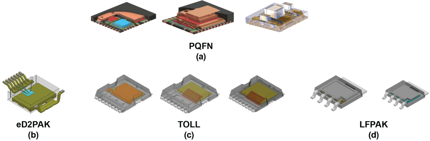
图1。Available power discrete capabilities include(一)PQFN进化,(二)eD2PAK with heat spreader tab,
(三)收费变化和(四)LFPAK.
为了最大限度地提高传统电源封装中的总导电率,源极和漏极需要连接到载流材料上,或接近模具设计中100%的可用空间。传统上,这是通过增加导线的数量,增加导线直径,或最大化连接到源极或漏极的夹子的大小来实现的。
从根本上改善电力sp的功能ace, three things must occur. First, the total conductivity from source and drain needs to be maximized. Second, thermal and electrical interfaces need to be eliminated or considerably reduced in length/thickness. Third, the conductive material density of the package needs to be increased. In the below figure, we examine the conductive density across a wide range of power-specific packaging in use today.
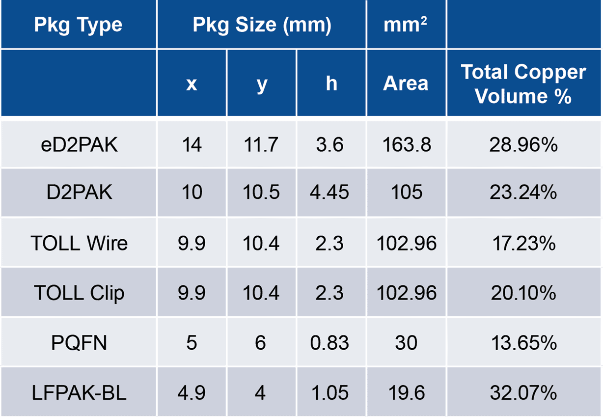
表1。现有电源包的比较数据。
为了最大限度地提高热性能和电性能,最好在封装体积内尽可能多地使用导电材料。在当今大多数电源封装中,封装中的导电材料很少超过25%(见表1)。
需要创建新的封装格式,以最大限度地提高封装中的导电密度。一个概念是PowerCSP™ Amkor开发的技术。PowerCSP技术的导电密度通常在40-70%的范围内,因此可以设计成比传统电源封装小得多的外形尺寸。这种增加是由于使用了连续的铜基板而不是夹子或导线。
 图3。PowerCSP的实现™ 技术显示了它的灵活性和许多施工方案。
In the PowerCSP technology, designs allow the die to use all the available source and drain area by connecting the die directly through a Cu pad that serves both as the current-carrying and heat-dissipating element. This results in lower resistance and inductance for the package compared to the group. Total package conductive density plays a factor, and also the use of the entire interface for source and drain to minimize potential losses in the system.
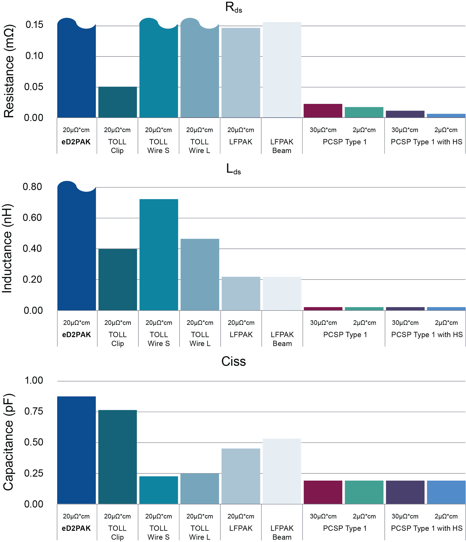
图7。PowerCSP中RDS、LDS和Ciss的模拟比较™ (PCSP)设计不同版本的eD2PAK、TOLL和LFPAK包.
其他封装概念可能是专门为电源开发的,但封装的导电密度将是一个关键因素。无论是Si、GaN还是SiC,都可以通过提高封装的导电密度来降低电阻、电感,最终降低封装本身的外形尺寸。努力提高封装的导电密度只能有助于解决封装的总功率密度问题,并使我们能够充分利用Si和WBG器件所能提供的所有优势。
关于作者
Shaun Bowers是亚利桑那州坦佩市Amkor Technology Inc.的主流高级封装集成副总裁。他于2000年加bob体彩入Amkor,目前负责汽车、引线框架和动力包装业务部门的包装开发。他曾担任技术项目管理、销售和客户服务等职务。在加入Amkor之前,他曾为Johnson Matthey Electronics和Honeywell Electronic Materials工作。他拥有冈萨加大学机械工程学位。
관련 게시물


코로나19업데이트(COVID-19)

48伏&
전력 패키징 트렌드