Increasing the Conductive Density of Packaging
Wide bandgap (WBG) semiconductor technologies have created new challenges and opportunities for power packages. Developments such as silicon carbide (SiC) and gallium nitride (GaN), have a higher figure of merit (FOM) compared to silicon MOSFETs and have extended the efficiency, output power and/or switching frequency range and operating temperature range for power electronics.
具有较低损耗,给定的尺寸功率器件可以控制更高的功率负载。例如,对于GaN功率晶体管,与基于硅的系统相比,电力系统可以具有¼尺寸,重量和效率损失。GaN技术可以解决从低功率(50W)端到中等甚至高功率水平的系统挑战,甚至在无线系统中等等。它在5G应用中的验收使其能够良好地用于复杂到中等电力包装。同样,SIC具有超出SI MOSFET的功率控制能力,需要为许多应用程序提供高级封装。WBG设备中的收益和优点需要新的封装选项来最大化整个电力系统的值。
Today’s discrete power packages are limited to the electrical performance of clip, wire and solder interfaces. In general, discrete packaging follows the design philosophy that greater size/volume correlates to higher power handling capability. However, these more efficient transistor technologies provide the ability to handle more power in the same size package or to reduce the form factor significantly.
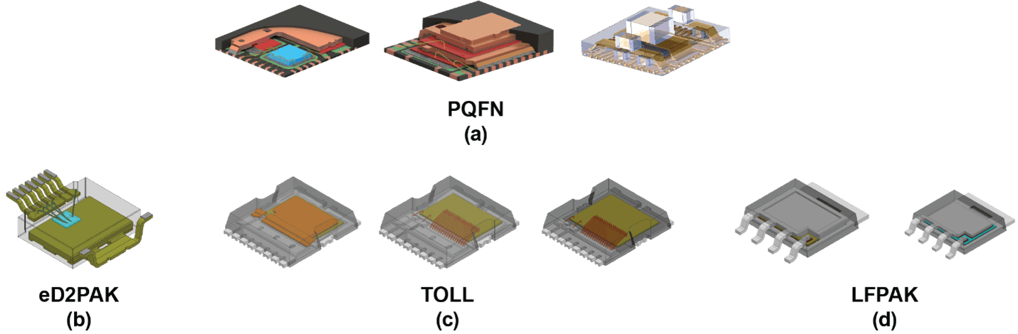
Figure 1.可用的电源离散功能包括(a)PQFN evolution,(b)ed2pak带散热器标签,
(c)TOLL variations and(d)LFPAK。
To maximize the total conductivity in traditional power packaging, the source and drain need to be connected to current carrying materials at or near 100% of the available space in the die design. Traditionally, this is done by increasing the number of wires, increasing the wire diameter, or maximizing the size of the clip attached to the source or drain.
为了从根本上改善电力空间中的功能,必须发生三件事。首先,需要最大化来自源和排水管的总电导率。第二,热和电界面需要在长度/厚度上消除或显着减小。第三,需要增加包装的导电材料密度。在下面的图中,我们在今天使用的各种功率特定包装中检查导电密度。
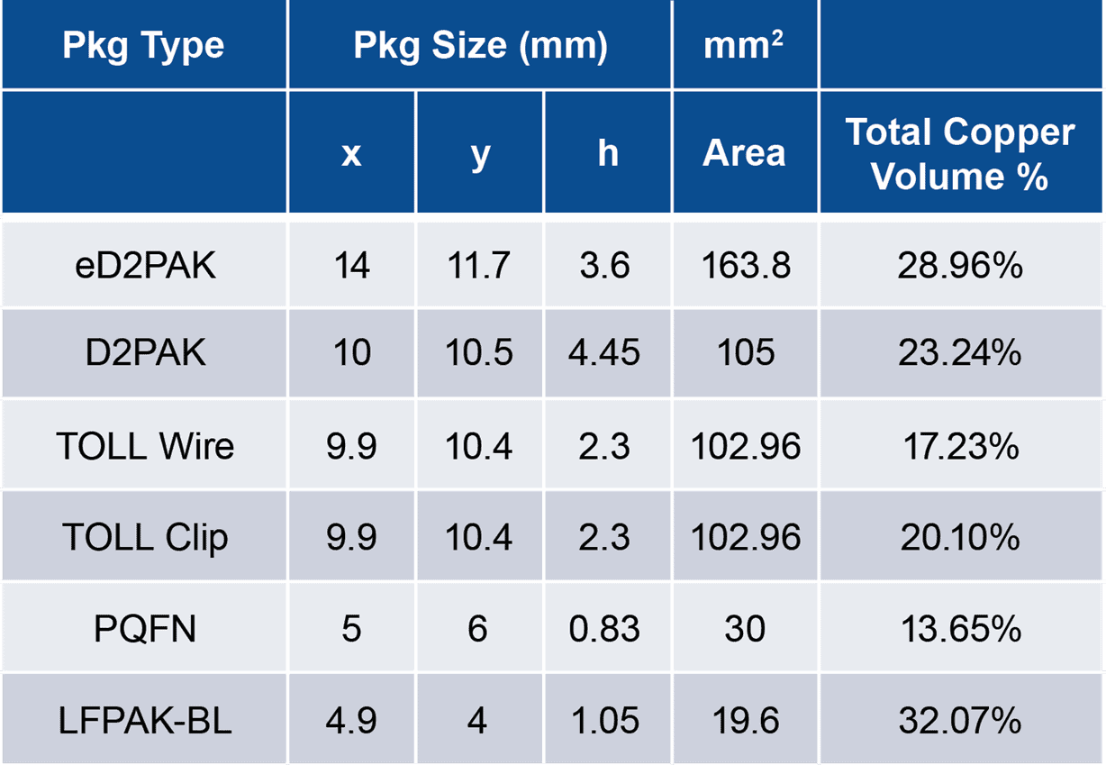
Table 1.Comparative data on existing power packages.
To maximize both the thermal and electrical properties, it would be preferred to have as much conductive material as possible within the volume of the package. In most power packaging today, the conductive material in the package rarely goes above 25% (refer to Table 1).
New package formats need to be created to maximize conductive density in the package. One concept is the PowerCSP™ technology developed by Amkor. PowerCSP technology is typically in the 40-70% range for conductive density and can be designed in a much smaller form factor than traditional power packages as a result. This increase is due to the use of a continuous Cu substrate instead of a clip or wires.
 Figure 2.PowerCSP™技术的实现显示了其灵活性和许多施工选项。
在PowerCSP技术中,设计允许模具通过直接通过作为电流承载和散热元件的Cu焊盘直接连接模具来使用所有可用的源和漏区。这导致与该组相比包装的耐耐电阻和电感。总封装导电密度起到一个因素,也是使用整个界面进行源极和排水物,以最大限度地减少系统中的潜在损失。
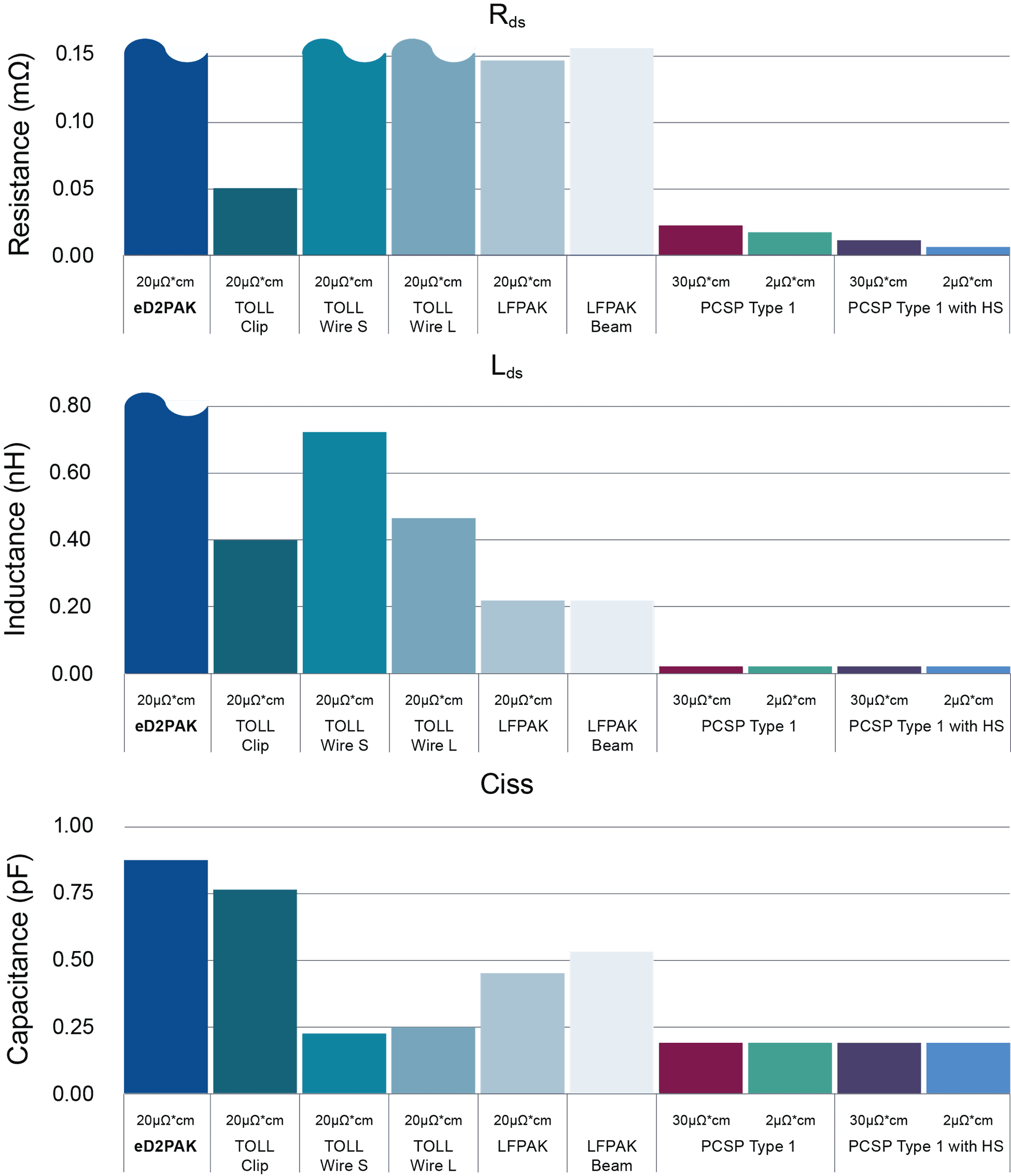
Figure 3.Simulated comparison of RDS, LDS and Ciss for the PowerCSP™ (PCSP) design to different versions of eD2PAK, TOLL and LFPAK packages.
Other package concepts might be developed specifically for power, but the conductive density of the package will be a key factor. Whether it is Si, GaN or SiC, all can benefit from increasing the conductive density of the package to lower resistance, inductance, and to ultimately reduce the form factor of the package itself. Efforts to increase the conductive density of the package can only help to address the overall power density of the package and allow us to take advantage of all that Si and WBG devices have to offer.
About the Author
肖恩鲍德斯is VP, Mainstream Advanced Package Integration at Amkor Technology Inc., Tempe, AZ. He joined Amkor in 2000 and is currently responsible for package development in automotive, leadframe and power packaging business segments. He previously held technical program management, sales and customer service roles as well. Prior to joining Amkor, he worked for Johnson Matthey Electronics and Honeywell Electronic Materials. He holds a degree in Mechanical Engineering from Gonzaga U.
Related Posts

Meeting the Challenges of 5G RF Production Test Services
bob体彩Amkor Technology中国通过Goodix Technology,Inc。认可